About Semiconductor
Manufacturing Processes
Tachibana’s Technology
Front-end Semiconductor Manufacturing Processes
Using Kumamoto’s abundant resources of clear groundwater, which contains extremely low levels of impurities, we are engaged in the manufacture of materials for the semiconductor industry, which requires advanced technology. Tachibana draws on its expertise in mixing and filtering technologies to collaborate with customers in manufacturing products for use in cutting-edge applications. Here, we give an overview of the materials used in upstream, front-end processes for semiconductor manufacturing.
Mask manufacturing process
Wafer manufacturing process
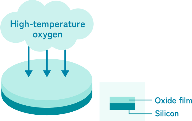
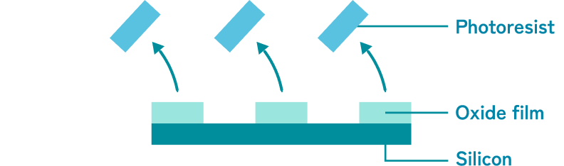
Process 01
Wafer surface oxidation
The process of oxidizing the surface of the wafer.
The oxide film acts as an insulating layer and forms a component of the transistor.
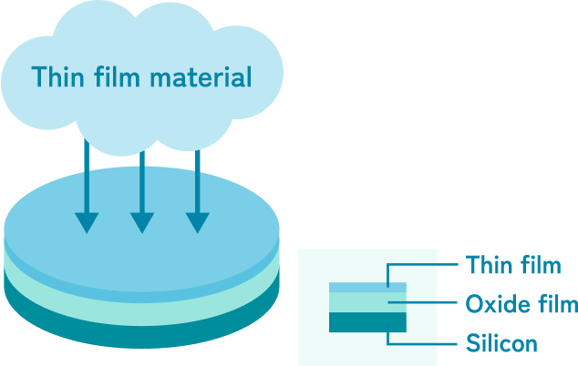
Process 02
Film deposition
The process of applying a thin film of material to the surface of the wafer.
Various deposition techniques are used.
Process 03
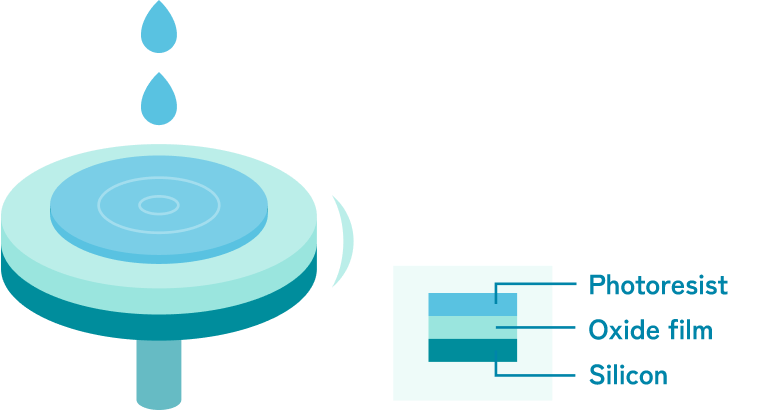
Photoresist coating
The process of applying a photosensitive material (photoresist) to the surface of the wafer.
The material differs depending on the type of light source used for exposure.
Tachibana’s Technology!
Top anti-reflection coating
Materials for reducing light reflection
Process 04
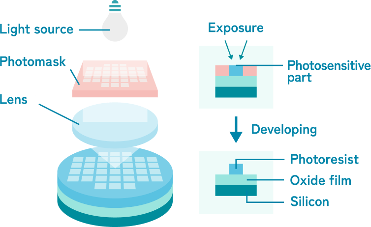
Exposure and developing
Circuit patterns are burned onto the wafer surface.
Then, any excess photoresist is removed with a developing solution.
Tachibana’s Technology!
Developing solution
Solution for excess unnecessary photoresist
Rinse agent
Supports cutting-edge EUV lithography
Shrink agent
Reduce the resist pattern size
Process 05

Etching
The oxide film and thin film are removed based on the pattern formed by the photoresist.
Process 06
Resist stripping and cleaning
The remaining photoresist is stripped off.
The wafer is immersed in a chemical solution to remove any remaining impurities.
Tachibana’s Technology!
Stripping solution
A solution for stripping off any remaining photoresist
Process 07
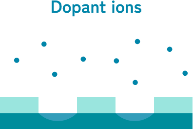
Ion implantation
Dopant ions are implanted, then activated with heat treatment.
Process 08

Flattening
A process of grinding the surface of a wafer to level out any unevenness.
Processes 03–08 are
repeated several times.
Process 09
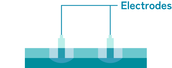
Electrode formation
Metal for electrode wiring is embedded in the wafer.
Process 10
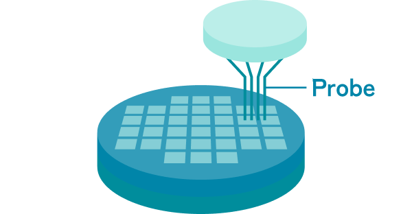
Wafer inspection
The chips formed on the wafer are inspected for electrical problems.